Imprimer la page
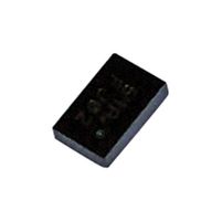
NCP451AFCT2G
Power Distribution Switch, Active High, 1 Output, 0.012 ohm On, 5.5 V, 3 A, WLCSP-6

L'image a des fins d'illustration uniquement. Veuillez lire la description du produit.


FabricantONSEMI
Réf. FabricantNCP451AFCT2GCopie
Délai d’approvisionnement standard du fabricant19 semaines
Code Commande
Bobine complète86X0822
Bandes découpées13AC6139
Votre numéro de pièce
Disponible sur commande
Délais d’approvisionnement standard du fabricant : 19 semaine(s)
Options de conditionnement
| Type de conditionnement | Quantité | PU HT: | Total |
|---|---|---|---|
| Bandes découpées | 3000 | 0,341 $ | 1 023,00 $ |
| Total Prix | 1 023,00 $ | ||
Bandes découpées
| Quantité | Prix |
|---|---|
| 3000+ | 0,341 $ |
Bobine complète
| Quantité | Prix |
|---|---|
| 3000+ | 0,410 $ |
| 6000+ | 0,378 $ |
| 12000+ | 0,354 $ |
| 18000+ | 0,330 $ |
| 30000+ | 0,315 $ |
Note à la ligne
Ajouté à votre confirmation de commande, à votre facture et à votre note d’expédition pour cette commande uniquement.
Informations produit
FabricantONSEMI
Réf. FabricantNCP451AFCT2GCopie
Délai d’approvisionnement standard du fabricant19 semaines
Code Commande
Bobine complète86X0822
Bandes découpées13AC6139
Fiche technique
Power Load Switch TypeHigh Side
No. of Channels1Channels
Input Voltage5.5V
Current Limit-
On State Resistance1mohm
IC Case / PackageWLCSP
No. of Pins6Pins
Thermal ProtectionYes
On / Enable Input PolarityActive High
No. of Outputs1Outputs
Operating Temperature Min-40°C
Operating Temperature Max85°C
Qualification-
Product Range-
MSL-
SVHCNo SVHC (25-Jun-2025)
Automotive Qualification Standard-
Distribution Switch Case StyleWLCSP
Aperçu du produit
NCP451AFCT2G is a 3A ultra-small low Ron and controlled load switch with an auto-discharge path. It is a very low Ron MOSFET controlled by an external logic pin, allowing optimization of battery life, and portable device autonomy. Indeed, due to a current consumption optimization with NMOS structure, leakage currents are eliminated by isolating the connected IC on the battery when not used. The output discharge path is also embedded to eliminate residual voltages on the output rail. Typical applications include mobile phones, tablets, digital cameras, GPS, and portable devices.
- Operational power supply range from 0.75 to 5.5V
- 12mohm N MOSFET from 3.6V to 5.5V, 13mohm N MOSFET from 1V to 3.3V
- DC current up to 3A, output auto discharge
- Active high EN pin
- Static drain-source on-state resistance is 12mohm typ (OUT = 200mA, TA = 25°C)
- Output discharge path is 1.2mohm typ (TA = + 25°C and VIN = 3.6V)
- Quiescent current is 8µA typ (VIN = 3.6V, TA = + 25°C)
- Output rise time is 670µs typ (RL = 10 ohm, COUT = 0.1µF, TA = + 25°C)
- Output fall time is 2.5µs typ (RL = 10 ohm, COUT = 0.1µF, TA = + 25°C)
- WLCSP6 package, ambient temperature range from -40 to +85°C
Spécifications techniques
Power Load Switch Type
High Side
Input Voltage
5.5V
On State Resistance
1mohm
No. of Pins
6Pins
On / Enable Input Polarity
Active High
Operating Temperature Min
-40°C
Qualification
-
MSL
-
Automotive Qualification Standard
-
No. of Channels
1Channels
Current Limit
-
IC Case / Package
WLCSP
Thermal Protection
Yes
No. of Outputs
1Outputs
Operating Temperature Max
85°C
Product Range
-
SVHC
No SVHC (25-Jun-2025)
Distribution Switch Case Style
WLCSP
Documents techniques (2)
Produits de remplacement pour NCP451AFCT2G
1 produit trouvé
Législation et Questions environnementales
US ECCN:EAR99
EU ECCN:Unknown
Conforme RoHS :Oui
RoHS
Conforme à la norme RoHS Phthalates:Oui
RoHS
SVHC :No SVHC (25-Jun-2025)
Télécharger le certificat de conformité du produit
Certificat de conformité du produit