Imprimer la page
5PB1104CMGI
CLOCK BUFFER, 200MHZ, DFN-8

L'image a des fins d'illustration uniquement. Veuillez lire la description du produit.
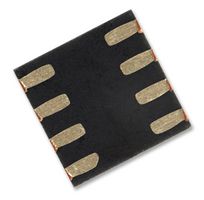


FabricantRENESAS
Réf. Fabricant5PB1104CMGICopie
Délai d’approvisionnement standard du fabricant35 semaines
Code Commande
Mise en bobine04AJ5824RL
Bandes découpées04AJ5824
Votre numéro de pièce
Disponible sur commande
Options de conditionnement
| Type de conditionnement | Quantité | PU HT: | Total |
|---|---|---|---|
| Bandes découpées | 1 | 3,710 $ | 3,71 $ |
| Total Prix | 3,71 $ | ||
Bandes découpées & Mise en bobine
| Quantité | Prix |
|---|---|
| 1+ | 3,710 $ |
| 50+ | 2,400 $ |
| 100+ | 2,120 $ |
| 250+ | 2,020 $ |
| 500+ | 1,900 $ |
| 1000+ | 1,850 $ |
| 2500+ | 1,800 $ |
| 5000+ | 1,780 $ |
Note à la ligne
Ajouté à votre confirmation de commande, à votre facture et à votre note d’expédition pour cette commande uniquement.
Informations produit
FabricantRENESAS
Réf. Fabricant5PB1104CMGICopie
Délai d’approvisionnement standard du fabricant35 semaines
Code Commande
Mise en bobine04AJ5824RL
Bandes découpées04AJ5824
Fiche technique
Clock IC TypeClock Buffer
Supply Voltage Min1.71V
Frequency200MHz
Supply Voltage Max3.465V
IC Case / PackageDFN
Clock IC Case StyleDFN
No. of Pins8Pins
Product Range-
Qualification-
No. of Outputs4Outputs
Operating Temperature Min-40°C
Operating Temperature Max85°C
SVHCNo SVHC (25-Jun-2025)
Aperçu du produit
5PB1104CMGI is a 5PB11xx series high-performance LVCMOS clock buffer. It has an additive phase jitter of 50fs RMS. There are five different fan-out variations available: 1:2 to 1:10. The 5PB11xx supports a synchronous glitch-free output enable (OE) function to eliminate any potential intermediate incorrect output clock cycles when enabling or disabling outputs. Typical applications include industrial applications automotive, radar, lidar, and other applications.
- High-performance 1:2, 1:4, 1:6, 1:8, 1:10 LVCMOS clock buffer
- Very low pin -to-pin skew: < 50ps
- Very low additive jitter: < 50fs
- Supply voltage range from 1.8V to 3.3V
- 3.3V tolerant input clock
- Maximum frequency of 200MHz
- Integrated serial termination for 50 ohm channel
- Available in 8 pin DFN package
- Temperature range from -40°C to +85°C
Spécifications techniques
Clock IC Type
Clock Buffer
Frequency
200MHz
IC Case / Package
DFN
No. of Pins
8Pins
Qualification
-
Operating Temperature Min
-40°C
MSL
MSL 1 - Unlimited
Supply Voltage Min
1.71V
Supply Voltage Max
3.465V
Clock IC Case Style
DFN
Product Range
-
No. of Outputs
4Outputs
Operating Temperature Max
85°C
SVHC
No SVHC (25-Jun-2025)
Documents techniques (2)
Législation et Questions environnementales
US ECCN:Unknown
EU ECCN:Unknown
Conforme RoHS :Oui
RoHS
Conforme à la norme RoHS Phthalates:Oui
RoHS
SVHC :No SVHC (25-Jun-2025)
Télécharger le certificat de conformité du produit
Certificat de conformité du produit