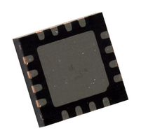
8P34S1102NLGI8
Fanout Buffer IC, 1.2GHz, 2 Outputs, 1.71V to 1.89V, -40°C to 85°C, VFQFN-16

| Type de conditionnement | Quantité | PU HT: | Total |
|---|---|---|---|
| Bandes découpées | 1 | 12,200 $ | 12,20 $ |
| Total Prix | 12,20 $ | ||
| Quantité | Prix |
|---|---|
| 1+ | 12,200 $ |
| 50+ | 8,810 $ |
| 100+ | 8,080 $ |
| 250+ | 7,660 $ |
| 500+ | 7,510 $ |
| 1000+ | 7,340 $ |
| 2500+ | 7,330 $ |
| 5000+ | 7,170 $ |
Informations produit
Aperçu du produit
8P34S1102NLGI8 is a high-performance differential LVDS fanout buffer. The device is designed for the fanout of 1PPS signals or high-frequency, very low additive phase-noise clock and data signals. The 8P34S1102 supports fail-safe operation and is characterized to operate from a 1.8V or 2.5V power supply. Guaranteed output-to-output and part-to-part skew characteristics make the 8P34S1102 ideal for those clock distribution applications demanding well-defined performance and repeatability. One differential input and two low skew outputs are available. The integrated bias voltage reference enables easy interfacing of single-ended signals to the differential device input. The device is optimized for low power consumption and low additive phase noise.
- Two low skew, low additive jitter LVDS output pairs
- One differential clock input pair
- Differential CLK, nCLK pairs can accept the following differential input levels: LVDS, CML
- Maximum input clock frequency of 51.2GHz
- Output skew of 3ps (typical), propagation delay of 400ps (maximum)
- Low additive phase jitter, RMS; fREF = 156.25MHz, 10kHz–20MHz: 34fs (typical)
- Device current consumption (IDD) of 40mA typical: 1.8V, 50mA typical: 2.5V
- Available in 16 pin VFQFN package
- Ambient operating temperature range from -40°C to 85°C
- Supports PCI Express Gen 1-5
Spécifications techniques
Fanout Buffer
Fanout Buffer
1.2GHz
2Outputs
1.89V
16Pins
-
85°C
No SVHC (25-Jun-2025)
Fanout Buffer
1.2GHz
VFQFN
1.71V
VFQFN
-
-40°C
MSL 3 - 168 hours
Documents techniques (2)
Législation et Questions environnementales
RoHS
RoHS
Certificat de conformité du produit